
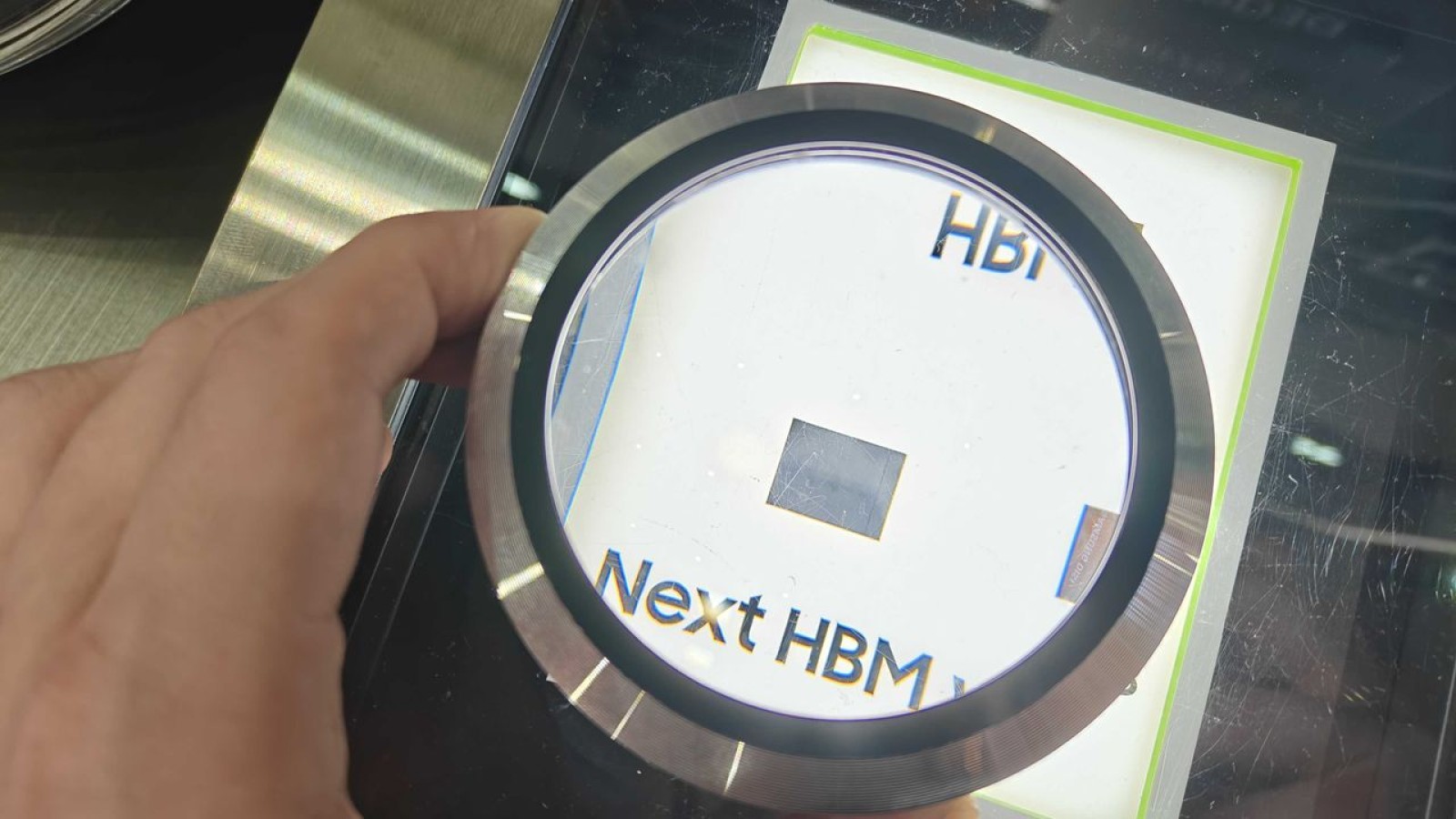
HBM5, the next-generation high-bandwidth memory standard now in development, is designed to double performance and improve power efficiency compared with HBM4E, Samsung revealed during the Memory Executive Summit held ahead of Semicon Taiwan 2026. Because doubling the data transfer rate of HBM4E within a single generation is not realistic, the company’s remarks suggest that HBM5 may instead double the number of interface pins to achieve the bandwidth increase.
According to Choi Jang-seok, head of product planning for the memory business at Samsung Electronics’ DS division, the target for HBM5 is to double performance while raising performance per watt by 20% over the HBM4E generation. Samsung has also previously stated that its HBM5 stacks will incorporate a heat path block (HPB) that lowers thermal resistance by 20% and simplifies cooling of the modules.
What Doubled Bandwidth Could Mean for AI Accelerators
Doubling per-stack memory bandwidth would push peak throughput to roughly 4 TB/s per stack in the 2028–2029 timeframe. TSMC anticipates that AI accelerators will adopt configurations of 20 to 24 HBM5/HBM5E stacks per package by the end of the decade. Those systems-in-packages would deliver aggregate memory bandwidth in the range of 80 TB/s to 96 TB/s within just a few years.
DRAM makers including Micron, Samsung, and SK hynix, along with controller and PHY developers such as Cadence, Rambus, and Synopsys, already offer HBM4/HBM4E controllers and interfaces rated for 16 GT/s. However, the official JEDEC transfer rate for HBM4E will land around 12 GT/s.
How Samsung Might Achieve the Performance Target
To deliver twice the bandwidth of HBM4E, the HBM5 specification would need to double the per-pin transfer rate from 12 GT/s to 24 GT/s, widen the interface from 2,048 to 4,096 bits, or combine a wider interface with a faster signaling rate. A 4,096-bit interface has already been floated by KAIST and Marvell, though that does not amount to any official confirmation of the specification’s target.
From a performance-per-watt standpoint, widening the interface is generally simpler than doubling the per-pin signaling rate. Higher per-pin speeds demand faster drivers, receivers, clocks, and equalization, along with tighter timing margins and a more sophisticated PHY, since maintaining signal integrity well beyond 20 GT/s is difficult. A wider interface moves more bits in parallel at a lower speed per wire, but expanding from 2,048 to 4,096 pins doubles the number of TSV and I/O paths, drivers, receivers, and bumps, while complicating routing and the base die.
As a result, a 4,096-I/O interface at moderate speed likely offers the best energy efficiency measured in picojoules per bit, yet the interface and package complexity could grow extreme enough to offset those gains. A 3,072-bit interface paired with a modest increase in data transfer rate could serve as a reasonable engineering comp
Source
Image: tomshardware.com